- Instant email delivery
- Global licenses
- Secure checkout
- 24/7 customer support
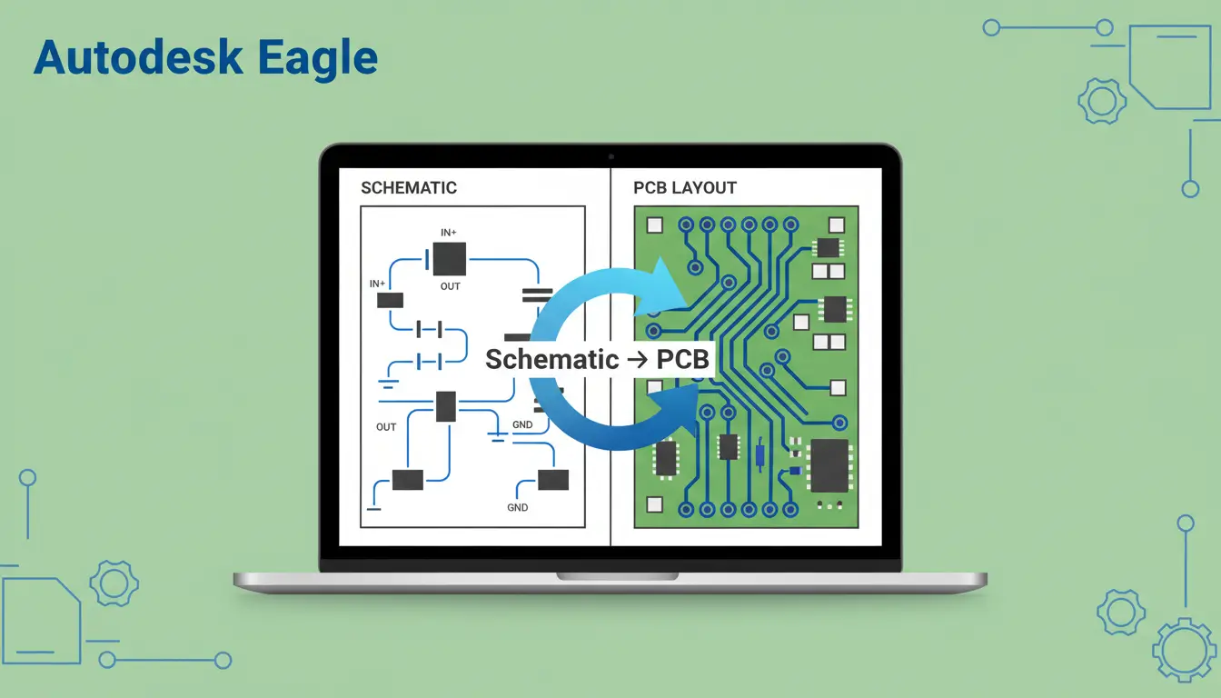
autodesk eagle is a compact, widely used PCB design application that balances power and approachability for hobbyists, makers, and small engineering teams. It combines schematic capture, component libraries, board layout, and CAM output in a single environment so you can move from concept to manufacturable files without stitching together multiple tools. Eagle excels when you need a lightweight, scriptable workflow for single- to multi-layer boards, quick prototype runs, or integration with mechanical design tools.
The basic workflow is straightforward: create a schematic to define connectivity, assign or create footprints, transfer the netlist to the board editor, place components thoughtfully, route signals by hand or with assisted routing tools, and run design rule checks before exporting Gerber and drill files for fabrication. Built-in features like ERC (electrical rule check), a robust parts library, and DRC (design rule check) make it practical for reliable results while keeping the learning curve moderate.
If you’re already using other Autodesk tools, Eagle’s ecosystem supports interoperability and data exchange—see the Autodesk software catalog for related products and bundles that can complement PCB work. Choose Eagle when you want a focused PCB tool that’s easy to learn, quick for iterative hardware development, and capable of producing industry-standard output for fabrication and assembly.
Start in the schematic editor: place parts, wire nets, annotate reference designators, and run ERC to catch connectivity issues. Next, generate or update the board from the schematic; arrange footprints with attention to signal flow, thermal considerations, and assembly constraints. Use interactive routing for critical nets and the autorouter for dense regions, then run DRC to validate clearances and layer rules. Finally, export Gerber, drill, and pick-and-place files for your board house and generate a BOM for procurement. For official downloads, licensing, and documentation visit the Autodesk official site to ensure you’re on the right version and license plan.
To get started, download the Eagle installer and required components from the Autodesk website and sign in with an Autodesk account. If you don’t have an account, create one during setup — it’s required to activate licenses and access trials. Choose the license type that fits your needs (subscription, educational, trial, or network) and the correct OS build. For a concise view of related Autodesk applications and bundles, see the Autodesk products overview.
Run the installer, accept permissions, and launch Eagle. When prompted, sign in using your Autodesk credentials so the app can fetch your license entitlement. Pick the release channel (stable vs. latest) and the build for your OS. For most users, a current stable 64‑bit build is best for libraries and CAM tool compatibility.
After activation, set workspace preferences: choose the Editor layout you prefer (board vs schematic), enable or collapse toolbars, and select a light or dark theme. Grid and snap are critical — turn on Display Grid and Snap to Grid, then set a primary grid that matches your design units (for PCB work start with 0.05 in or 1 mm grid and a finer snap of 0.01 in / 0.25 mm as needed). Save these settings as your default profile so new projects inherit them. For official installer details and account help, consult the Autodesk website.
autodesk eagle projects work best when libraries and search paths are deliberate. Start by creating a new project and placing a dedicated folder for its libraries so symbols, packages, and device sets stay together. Add existing component libraries to the project or create a new library when you need custom parts.
Organize libraries with a simple naming convention, then set library search paths so Eagle finds parts automatically when you draw schematics. Use the library manager or preferences to add your project folder and any shared library locations to the global search path. When you create a custom component, include clear device names and link footprints to avoid ambiguity later.
Keep a short checklist: create project folder, add or build libraries, register search paths, test by placing a part in a schematic. For broader Autodesk resources, see Autodesk software offerings and consult the official Autodesk site for product documentation and updates.
autodesk eagle schematic capture is a predictable, layout-driven process: open a new schematic, search component libraries, drop symbols, and connect them with labeled nets. Start a fresh sheet, set your grid and units, then use the library browser to find parts by name, function, or manufacturer. Place parts one at a time, orienting and snapping them to the grid so the later PCB layout stays tidy.
When you place a part, immediately assign its value (resistance, capacitance, IC part number) and choose the correct footprint or package variant. Use the attribute editor to add manufacturer and part numbers to reduce BOM confusion. If a symbol has multiple gates, invoke the remaining gates from the same device rather than placing separate components.
Organize signals with net labels and buses: name power rails (VCC, GND), label critical nets (RESET, SDA, SCL), and use hierarchical or global labels for multi-sheet projects. Proper net naming keeps the rat’s nest readable and simplifies ERC checks. Before leaving the schematic, run the Electrical Rule Check and resolve warnings; then synchronize nets to the PCB editor. For downloads and bundles related to Autodesk tools, see the Autodesk product collection.
Open a new schematic, use the “ADD” dialog to search libraries, and place components. After dropping parts, press R to rotate or M to move; use INVOKE to access alternate gates. Double-click a part to edit its value and footprint, and use the NAME tool to apply net labels or create buses. For power nets, place a single power symbol and label all references with the same net name to ensure connectivity across sheets. Regularly run ERC and visually inspect the rat’s nest for stray connections. When symbols are finalized, generate a BOM and prepare a netlist for PCB layout; for official product details, visit the Autodesk product pages.
Annotating your schematic in Autodesk Eagle is a crucial early step: assign unique designators, then visually confirm pin-to-pin connections by drawing nets between component pins. Add explicit power symbols and place connectors where harnesses or board edges interface with other systems.
ERC commonly finds unconnected pins, conflicting net names, missing power pins, and accidental shorts. For each error, trace the net, confirm the device pin type (PWRIN/PWROUT), and update net names or add explicit jumpers. Repeat ERC after fixes until warnings are acceptable. For software details and downloads, see the Autodesk official site and our Autodesk software listings.
In autodesk eagle, switch to Board view or generate a board directly from your schematic to begin the PCB layout workflow. Use the schematic’s “Switch to Board” or “Update Board” action so components and nets are transferred as a ratsnest; footprints and net names remain synchronized. Define the board outline early by drawing the mechanical shape on the appropriate layer and locking it, then set a sensible grid to control placement. Move critical parts first, place decoupling capacitors close to power pins, and reserve space for mounting holes and connectors. Run ERC/DRC regularly during layout to catch library mismatches and clearance issues. For related Autodesk tools and resources, see the Autodesk software page.
autodesk eagle makes the schematic-to-board transfer straightforward. After creating or opening a board, the transfer action adds components to the canvas with nets intact so you can begin placement immediately. Draw the board outline (Wire/Dimension layer), set an appropriate grid, then group parts by function and keep sensitive or high-speed nets short. Use the Invoke dialog to select alternate packages if a symbol supports multiple footprints. Route power and ground planes early, use via stitching where needed, and collapse overlapping elements. Periodically run ERC/DRC and update the schematic when changing references. When layout is verified, generate Gerbers and manufacturing files; for official product documentation visit the Autodesk official site.
Before routing, arrange components to favor manufacturability: group by function, orient polarized parts consistently, and place high-pin-count or heat-generating parts to minimize long traces. Define the board outline and mechanical keep-out areas early so placement respects connectors, mounting holes, and enclosure fit.
Finalize dimensions, lock component placement, and run a full DRC. For tool-specific workflows and downloads, see the Autodesk software downloads. For official product guidance and best practices, consult Autodesk product pages.
autodesk eagle users should decide early whether to route manually or use the autorouter. Manual routing gives control over trace topology, impedance and cleanup; an auto-router speeds completion on dense boards but may require heavy cleanup of vias and detours. Begin by defining your design rules: set minimum and target trace widths for power, digital, and high-speed nets; specify via types (through-hole, blind, microvia) and their drill annular ring limits. Route critical nets first — power, ground returns and high-speed differential pairs — keeping them on continuous layers and maintaining consistent trace width for controlled impedance. Use plane layers for power and ground when possible and stitch with multiple vias to lower impedance. For vias, choose plated through vias for reliability, microvias for fine-pitch BGA escape, and consider dogbone or thermal reliefs for heat-sensitive pads. Use push-and-shove and follow-me features for interactive manual routing to maintain spacing and clearance automatically. After routing, run DRC and impedance checks, then clean up unnecessary vias and serpentine segments. Document any layer swaps or blind via usage for fabrication. If you rely on automation, set the router constraints tightly and route critical nets manually first so the auto-router focuses on less-sensitive signals. For more on tool workflows see the Autodesk product pages.
autodesk eagle provides both an autorouter and robust interactive routing tools. Start by setting board Design Rules (DRC) — trace widths, via sizes and layer stack — so both manual and auto modes respect impedance and spacing. Route power and high-speed nets manually first, then run the autorouter for remaining signals with tight constraints. Use the route tool’s follow-me and push commands to preserve clearances and to easily add teardrops or thermal spokes for power vias. For BGA escape, plan layer transitions and microvia placement early. After routing, run a DRC and use the ratsnest to verify connections. If you need downloads, consult the Autodesk official site for the latest Eagle updates and documentation. Avoid 90° bends on high-speed traces, keep differential pairs symmetrical and use serpentine length tuning where necessary. Finally, generate fabrication notes and CAM outputs to communicate via types and layer stack to your manufacturer.
A reliable DRC and validation flow is essential to catch clearance, drill and copper problems before boards go to fabrication. Start by defining net-specific clearances, minimum annular ring and drill sizes, and copper-to-copper spacing for signal, power and plane layers. Configure rules for via-to-pad annular rings, microvia and plated through-hole drills, and pour isolation so copper pours don’t create unintended shorts. Include fabrication constraints such as minimum track width, solder mask expansion and keepout regions for mechanical features or test points.
Run the DRC iteratively and treat the report as a prioritized checklist: fix errors related to shorted nets and broken connections first, then address marginal clearances and manufacturability flags. Use cross-probing to link violations back to the schematic and footprints to decide whether to adjust routing, pad geometries, or rule parameters. After corrections, re-run DRC until no critical violations remain. Finally, validate outputs by generating Gerber and drill files and performing a CAM check; this last step catches issues like excessive thermal reliefs or silkscreen overlaps that the DRC might not flag.
For tool compatibility and licensing guidance refer to SoftAuthentic’s Autodesk software offerings and the official Autodesk site for product documentation and manufacturing best practices.
In Autodesk Eagle, begin DRC setup by selecting the Clearances, Sizes and Layers tabs in the DRC dialog. Set a conservative global clearance, then override for sensitive nets (e.g., high-voltage or high-current). Specify hole-to-pad annular ring minima and define a drill tool list that matches your manufacturer’s capabilities. Use copper pour and thermals settings to control plane behavior and avoid isolated islands.
Run DRC and inspect markers; use the error list to navigate to each violation and decide whether to relax rules, adjust routing or modify footprints. After fixes, run an electrical rule check (ERC) and a final DRC pass to ensure the board is production-ready.
autodesk eagle simplifies the technical steps of preparing fabrication and assembly outputs, but attention to detail prevents costly re-spins. Begin by confirming layer mapping and running the CAM processor to produce RS-274X Gerber files and an Excellon drill file. Set apertures, soldermask, paste and mechanical layer assignments explicitly, and choose consistent units and zero-suppression for drills. Export a Bill of Materials that includes reference designators, quantities, manufacturer part numbers and footprints, and create pick-and-place (XY) data that preserves rotation and polarity. Name files clearly and bundle them into a single archive. Before submission, run a final DRC and preview the outputs in a Gerber viewer to check for flipped layers, missing apertures, incorrect board outlines or mask issues. If you need more Autodesk product options and licensing, see the SoftAuthentic Autodesk overview.
Keep the export process reproducible: use a saved CAM job for Gerbers and a consistent CSV template for the BOM. For assembly, include a separate pick-and-place file with origin specification and units, and attach a simple fabrication note stating board thickness, finish and impedance if relevant. Verify top and bottom copper, silkscreen, soldermask, mechanical layers and edge cuts are present and correctly ordered. Run a visual layer-stack check with a Gerber viewer and confirm drill-to-pad alignment. Share the ZIP archive and a short README with your fabricator to prevent misunderstandings. For official guidance on Autodesk manufacturing workflows, consult the Autodesk Product Design & Manufacturing overview.
If you designed in autodesk eagle, get ahead of delays by supplying clear fabrication files and a concise readme. Export Gerber RS-274X, NC drill, assembly (centroid) and pick-and-place files, plus a BOM and an annotated silkscreen PDF. Specify finish (ENIG recommended), soldermask color, and minimum trace/space and annular ring requirements.
Panelization & tooling hints: provide a panel drawing or request the fab’s preferred panel array; include fiducials and tooling holes, keep a 5 mm rail and 0.5 mm edge clearance, and indicate V-groove or mouse-bite routing. For SMT stencils, include paste and component height notes for assembly.
Recommended layer stackup (communicate with your board house): for 2-layer use 1.6 mm FR‑4, 1 oz Cu; for 4-layer use a signal–plane–plane–signal arrangement with 1 oz copper and manufacturer default prepreg thicknesses. When in doubt, link your files to your fabricator and consult their DFM checklist.



 Autodesk
 Design Softwares
 CorelDraw
 Affinity V2
 Microsoft & Windows
 Windows
 Microsoft 365